Introduction
Electrostatic discharge (ESD) remains one of the most critical and underestimated reliability challenges in modern electronics. As semiconductor technologies continue to scale toward smaller geometries and higher integration densities, electronic systems become increasingly vulnerable to transient electrical events.
A single ESD event can permanently damage integrated circuits, degrade system reliability, corrupt data, trigger unintended behavior, or even create latent failures that appear months after deployment.
Today’s electronic ecosystem is far more complex than ever before. Modern products integrate:
- High-speed digital systems
- AI processors
- Advanced CMOS technologies
- Power electronics
- Automotive electronics
- IoT devices
- Medical wearables
- RF communication systems
- Satellite communication equipment
- Industrial automation systems
- Bio-signal-driven robotics
As a result, ESD protection is no longer simply a manufacturing concern — it has become a fundamental design, compliance, EMC, safety, and reliability issue.
Recent developments in international standards, advanced semiconductor technologies, medical electronics, wearable robotics, automotive systems, and power electronics are rapidly reshaping how engineers approach ESD immunity and protection.
This article explores the latest developments in ESD science, standards, regulations, testing methodologies, protection strategies, emerging applications, and future industry challenges.
Understanding Electrostatic Discharge (ESD)
Electrostatic discharge is the sudden transfer of electrostatic charge between objects with different electrical potentials.
ESD events may occur through:
- Human contact
- Automated manufacturing equipment
- Cable discharge events
- Charged devices
- Switching transients
- Environmental charging
- Friction (triboelectric charging)
Even though ESD events may involve extremely small energies, their voltage levels can reach several kilovolts.
Typical ESD Sources
| Source | Typical Voltage |
|---|---|
| Walking on carpet | 1 kV – 35 kV |
| Plastic handling | 1 kV – 20 kV |
| Human body discharge | 2 kV – 15 kV |
| Automated handling systems | Hundreds of volts to several kV |
| Cable discharge events | High transient currents |
Modern semiconductor devices with nanometer-scale gate oxides can be damaged by voltages far below traditional ESD thresholds.
Why ESD Is Becoming More Critical
Historically, older bipolar technologies were relatively robust against ESD stress.
Today, modern semiconductor technologies present dramatically reduced ESD margins due to:
- Ultra-thin gate oxides
- Lower operating voltages
- Higher integration density
- Smaller geometries
- Advanced packaging technologies
- High-speed interfaces
- Increased sensitivity of RF circuits
According to recent IEEE research, shrinking CMOS technologies continue to reduce gate oxide breakdown voltages, significantly tightening the ESD design window.
Modern Technologies Vulnerable to ESD
| Technology | ESD Challenge |
|---|---|
| FinFET | Reduced voltage margins |
| GAA Transistors | Complex current paths |
| 3D ICs | Thermal and discharge complexity |
| Chiplets | Interconnect vulnerability |
| RF Front Ends | Low-capacitance protection required |
| AI Accelerators | Dense high-speed interconnects |
| Wide-Bandgap Devices | High-energy transient sensitivity |
This trend makes advanced ESD engineering essential for all modern electronic products.
Physics of ESD Events
ESD is fundamentally a transient electromagnetic phenomenon.
During discharge:
- Current rises extremely rapidly
- Voltage spikes appear across sensitive nodes
- Localized heating occurs
- Junction breakdown may occur
- Metal interconnects may melt
- Gate oxides may rupture
Some ESD events generate current rise times below one nanosecond.
Common ESD Failure Mechanisms
| Failure Mechanism | Description |
|---|---|
| Gate Oxide Breakdown | Permanent dielectric damage |
| Junction Melting | Localized thermal destruction |
| Metal Migration | Interconnect degradation |
| Latch-Up | Parasitic SCR triggering |
| Latent Damage | Hidden long-term reliability degradation |
| Soft Failure | Temporary malfunction or reset |
Latent failures are especially dangerous because systems may initially pass functional tests but fail later in the field.
Standardized ESD Test Models
To ensure repeatable qualification, several industry-standard ESD models have been developed.
Human Body Model (HBM)
HBM simulates a human discharging into an electronic device.
Typical equivalent circuit:
- 100 pF capacitor
- 1.5 kΩ resistor
HBM remains one of the most widely used qualification standards.
According to recent IEEE literature, a 2 kV HBM event can generate peak currents around 1.3 A.
Charged Device Model (CDM)
CDM represents the case where the device itself becomes charged and discharges upon contact with ground.
CDM is now considered one of the most critical threats for advanced semiconductor technologies because:
- Rise times are extremely fast
- Peak currents are very high
- Advanced nodes are highly sensitive
A 500 V CDM event may produce currents exceeding 7 A with rise times below 250 ps.
Machine Model (MM)
The Machine Model simulates discharge from metallic handling equipment.
Although MM is less emphasized today, it historically represented automated manufacturing risks.
Human Metal Model (HMM)
HMM is becoming increasingly important for system-level testing.
It represents:
- Human interaction with metallic interfaces
- System-level transient events
- Real-world user interactions
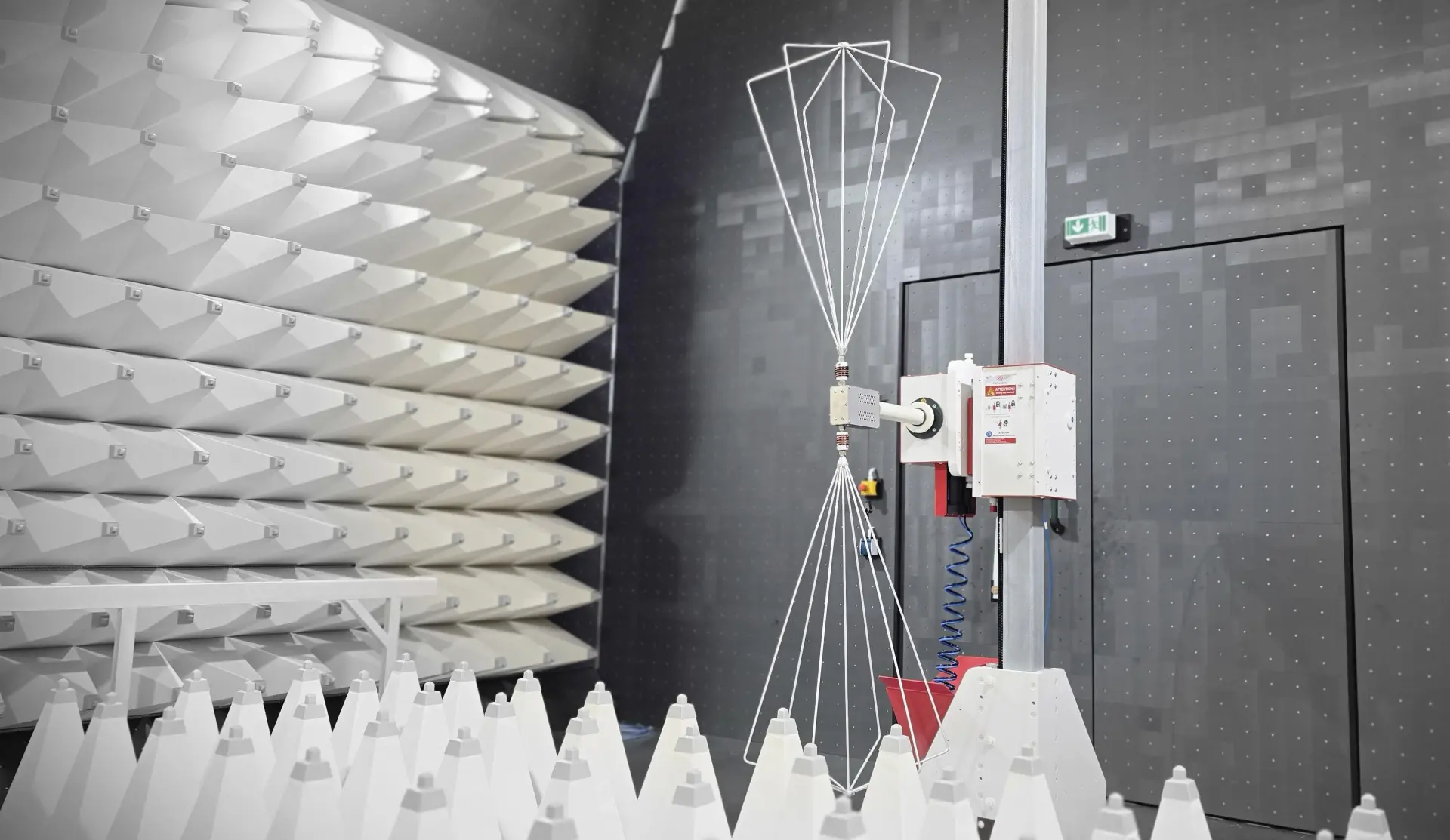
IEC 61000-4-2 and the New 2025 Standard Evolution
One of the most important ESD immunity standards globally is IEC 61000-4-2.
The latest revision, EN 61000-4-2:2025, introduces major updates reflecting modern electronic environments and technologies.
Major Updates in EN 61000-4-2:2025
Enhanced Voltage Levels
| Severity Level | Contact Discharge | Air Discharge |
|---|---|---|
| Level 1 | 2 kV | 2 kV |
| Level 2 | 4 kV | 4 kV |
| Level 3 | 6 kV | 8 kV |
| Level 4 | 8 kV | 15 kV |
| Level X | Custom | Custom |
The 2025 revision introduces:
- Higher test voltages
- Improved waveform verification
- Updated coupling plane methodologies
- Better environmental conditioning guidance
- Clarified performance criteria
- Expanded coverage for IoT and wearable devices
ESD in Medical Electronics and Wearable Technologies
One of the most fascinating emerging ESD research areas involves bio-signal-driven wearable devices and medical robotics.
Modern wearable medical systems rely on:
- Electromyogram (EMG) signals
- Electroencephalogram (EEG) signals
- Bio-signal sensors
- Wireless communication links
- Human-machine interfaces
According to IEEE EMC Magazine research, these systems require extremely high immunity against electromagnetic disturbances because even minor interference can corrupt weak biological signals.
Challenges in Bio-Signal Wearable Devices
| Challenge | Description |
|---|---|
| Extremely Weak Signals | µV/mV signal levels |
| Human Body Coupling | Complex EMC interactions |
| Reproducibility | Difficult testing conditions |
| Safety Requirements | Critical human interaction |
| Wireless Connectivity | Additional EMC paths |
Researchers recently proposed advanced ESD immunity test systems using:
- Bio-equivalent phantoms
- Simulated EMG generators
- Stable artificial bio-signals
- Controlled ESD injection methodologies
These techniques improve repeatability and may eventually influence future international standards for wearable robotics and biomedical EMC testing.
ESD in Automotive Electronics
Modern vehicles contain hundreds of electronic control units (ECUs), high-speed communication buses, sensors, power electronics, and AI-driven systems.
This dramatically increases ESD exposure risks.
Automotive ESD Challenges
| System | ESD Concern |
|---|---|
| ADAS Systems | Sensor reliability |
| Battery Management Systems | High-voltage transients |
| Infotainment | User interface exposure |
| Radar Systems | RF sensitivity |
| Ethernet Automotive Networks | High-speed signal integrity |
| EV Charging Systems | Surge and ESD exposure |
Automotive standards increasingly require:
- Higher immunity levels
- Functional safety compliance
- System-level transient robustness
- Extended qualification cycles
ESD Protection in Power Electronics
Power electronics represent another rapidly evolving ESD challenge.
According to IEEE Power Electronics Magazine, modern power systems increasingly employ highly sensitive CMOS and MOSFET-based architectures vulnerable to ESD and transient events.
Applications affected include:
- Industrial converters
- Telecom infrastructure
- Medical power supplies
- Renewable energy systems
- LED lighting systems
- EV chargers
- Data center power systems
Why Power Electronics Are Vulnerable
| Factor | Impact |
|---|---|
| High Power Density | Thermal stress |
| Fast Switching | Transient generation |
| Harsh Environments | Increased surge exposure |
| Wide-Bandgap Devices | Sensitive gate structures |
| Long Cable Runs | Induced transient energy |
Modern standards increasingly require compliance with:
- IEC 61000-4-2
- IEC 61000-4-4
- IEC 61000-4-5
- IEC 55035
- IEC 60601-1-2
Recent approaches include using automotive-qualified ESD-capable rectifiers directly within power converter architectures.
Advanced On-Chip ESD Protection Structures
Advanced On-Chip ESD Protection Structures
Modern ICs use sophisticated on-chip ESD protection structures.
Common ESD Protection Devices
| Device Type | Advantages | Challenges |
|---|---|---|
| Diodes | Simple, low leakage | Limited robustness |
| MOS Clamps | Good integration | Area consumption |
| SCR Structures | High robustness | Latch-up risk |
| TVS Devices | Fast response | Capacitance concerns |
| Rail Clamps | System-wide protection | Trigger optimization |
According to recent IEEE research, the coordination between I/O protection structures and power-rail clamps is essential for effective discharge path formation.
The ESD Design Window
One of the most important modern ESD design concepts is the ESD design window.
The protection device must:
- Trigger above normal operating voltage
- Clamp below gate oxide breakdown voltage
As technologies scale, this window becomes increasingly narrow.
ESD Design Window Constraints
| Parameter | Requirement |
|---|---|
| Trigger Voltage | Above supply voltage |
| Holding Voltage | Avoid latch-up |
| Clamp Voltage | Below oxide breakdown |
| Leakage | Minimal during operation |
| Capacitance | Compatible with high-speed signals |
Advanced nodes make these tradeoffs extremely challenging.
Latch-Up and ESD Interactions
Latch-up remains one of the most dangerous ESD-related reliability phenomena.
Parasitic silicon-controlled rectifiers (SCRs) inside CMOS structures can accidentally trigger during ESD events.
Consequences include:
- Excessive current conduction
- Thermal runaway
- Permanent damage
- System destruction
Modern ESD design must therefore carefully balance:
- ESD robustness
- Latch-up immunity
- Performance
- Area efficiency
ESD Challenges in High-Speed and RF Systems
Modern high-speed interfaces present major ESD protection difficulties.
Interfaces include:
- USB4
- PCIe Gen6
- 112G SerDes
- Automotive Ethernet
- mmWave systems
- RF front ends
High-Speed ESD Design Challenges
| Challenge | Description |
|---|---|
| Low Capacitance Requirements | Signal integrity preservation |
| Fast Rise Times | Limited clamp activation time |
| RF Loss | Protection parasitics |
| Packaging Effects | Complex current paths |
| Multi-Gigabit Data Rates | Timing sensitivity |
Designers increasingly use:
- Ultra-low capacitance TVS devices
- Distributed protection architectures
- Co-design approaches
- Electromagnetic simulation
AI, IoT, and Future ESD Challenges
Emerging technologies are introducing entirely new ESD concerns.
AI Systems
AI accelerators contain:
- Massive interconnect densities
- High-speed memory interfaces
- Extremely sensitive nodes
Even small ESD-induced disturbances may impact:
- AI training reliability
- Data integrity
- Edge AI performance
IoT Ecosystems
IoT devices face unique ESD risks because they are:
- Highly distributed
- Frequently user-accessible
- Battery powered
- Connected wirelessly
- Often deployed in harsh environments
The 2025 IEC revisions now explicitly address connected devices and IoT applications.
System-Level ESD Testing
Component-level qualification alone is no longer sufficient.
System-level ESD testing evaluates:
- Real-world user interactions
- Cable discharge events
- Connector exposure
- Chassis coupling
- Grounding effectiveness
System-Level Test Areas
| Test Area | Purpose |
|---|---|
| Direct Contact Discharge | User touch simulation |
| Air Discharge | Realistic environmental events |
| Coupling Plane Tests | Indirect transient coupling |
| Cable Injection | Connector robustness |
| Functional Monitoring | System behavior validation |
System-level immunity is becoming increasingly important for:
- Medical devices
- Automotive systems
- Telecom infrastructure
- Industrial automation
- Aerospace systems
ESD Control in Manufacturing
Manufacturing environments require strict ESD control programs.
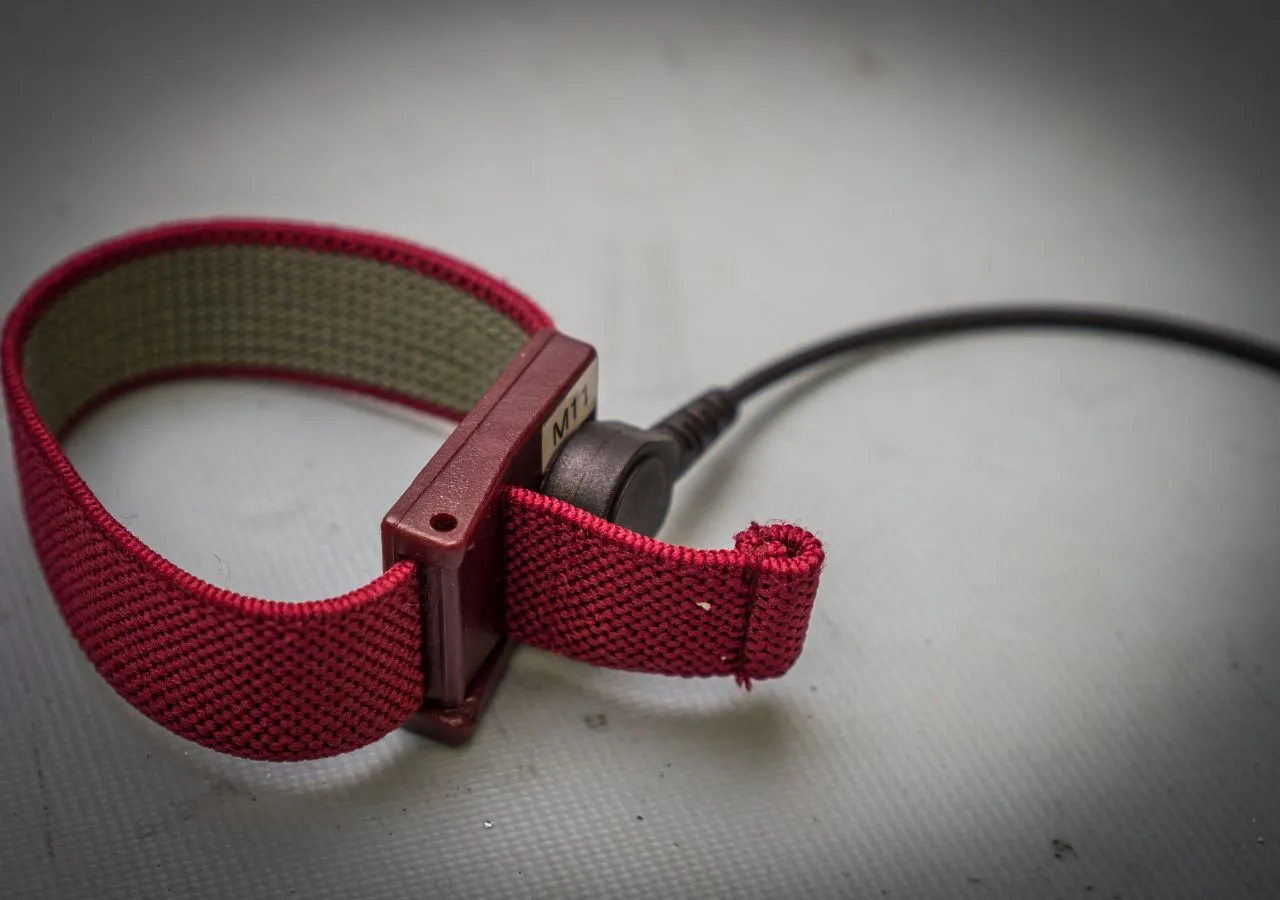
Common ESD Control Measures
| Control Method | Purpose |
|---|---|
| Grounded Workstations | Charge dissipation |
| Conductive Flooring | Personnel grounding |
| Wrist Straps | Human charge equalization |
| Ionizers | Neutralization of insulators |
| ESD Packaging | Safe transportation |
| Humidity Control | Reduced static generation |
Poor ESD control may cause:
- Immediate device failure
- Latent damage
- Yield reduction
- Increased warranty returns
Future Trends in ESD Engineering
The future of ESD engineering will likely involve:
- AI-assisted protection design
- Real-time transient monitoring
- Smart self-healing protection circuits
- Advanced simulation-based optimization
- Protection for sub-THz systems
- Quantum electronics ESD protection
- Bio-integrated electronics immunity
Future Research Areas
| Area | Importance |
|---|---|
| 3D IC ESD Modeling | Advanced packaging |
| Chiplet Protection | Heterogeneous integration |
| Wearable Medical EMC | Human interaction |
| AI-Optimized ESD Design | Autonomous optimization |
| Quantum Electronics Protection | Emerging technologies |
The evolution of ESD engineering is increasingly interdisciplinary, involving:
- Electromagnetics
- Semiconductor physics
- Circuit design
- Reliability engineering
- Biomedical engineering
- AI-assisted modeling
Conclusion
Electrostatic discharge remains one of the most critical reliability and EMC challenges in modern electronics.
As semiconductor technologies scale and electronic systems become increasingly interconnected, ESD protection is evolving far beyond traditional manufacturing concerns.
Modern ESD engineering now intersects with:
- AI systems
- Wearable robotics
- Biomedical devices
- Automotive electronics
- Power electronics
- IoT ecosystems
- Advanced semiconductor technologies
- High-speed communication systems
Recent updates such as EN 61000-4-2:2025 demonstrate how regulatory frameworks are evolving to address modern technological realities.
At the same time, emerging research on wearable robotics, advanced CMOS protection, system-level immunity, and AI-driven electronics is reshaping the future of EMC and reliability engineering.
For engineers, manufacturers, testing laboratories, and product developers, understanding modern ESD challenges is no longer optional — it is essential for ensuring product reliability, compliance, safety, and long-term operational success.
References
- IEC 61000-4-2:2024 / EN 61000-4-2:2025.
- Chun-Yu Lin and Ming-Dou Ker, “ESD Protection Design: Fundamentals and Advanced Strategies,” IEEE Open Journal of the Solid-State Circuits Society, 2026.
- Jianqing Wang, “ESD Immunity Test System for Bio-Signal-Driven Wearable Robots,” IEEE EMC Magazine, 2024.
- Kevin Parmenter, “ESD Protection for Power Electronic ICs and Discrete Devices,” IEEE Power Electronics Magazine, 2024.
- JEDEC JESD22-A114 Human Body Model.
- JEDEC JESD22-C101 Charged Device Model.
- IEC 60601-1-2 Medical EMC Standard.
- IEC 61000-4-5 Surge Immunity Standard.
- Automotive Electronics Council (AEC) ESD Qualification Standards.
- CISPR and IEC TC77 EMC standardization activities.
At Stancer Testing Lab, we support manufacturers with practical EMC and ESD testing services for product compliance, reliability evaluation, and design troubleshooting.
Related Articles