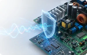


Key Reasons for EMC test failure
Why Electronic Products Fail EMC and RF Compliance Testing
You can spend months developing a product that works perfectly on the bench, performs well during internal validation, and meets every functional requirement, only to see it fail decisively during compliance testing. The unit powers on, communicates, measures, charges, switches, or transmits exactly as intended. Then it enters the chamber and the emissions plot crosses the limit line. Or the product is exposed to an immunity test and suddenly resets, freezes, loses data, or behaves unpredictably.
This situation is frustrating, but it is rarely random. Most EMC failures are rooted in predictable design choices: switching power supplies with large current loops, high-speed signals without controlled return paths, long cables acting as antennas, insufficient filtering, poor enclosure bonding, noisy clock sources, or wireless modules integrated without considering the final host environment.
That is why successful compliance is not something that should begin at the end of development. It should be built into schematic design, PCB layout, enclosure design, cable routing, firmware test modes, and system validation from the beginning. Structured EMC testing, early EMC pre-compliance testing, and practical RF testing services help engineering teams identify risk long before formal certification begins.
Engineering insight: A product that functions correctly is not automatically compliant. Functional validation proves the circuit performs its intended task. EMC validation proves the product performs that task without creating excessive electromagnetic disturbance and without becoming vulnerable to electromagnetic stress.
Why Working Prototypes Still Fail Compliance Testing
Many EMC problems are invisible during normal bench testing. A digital interface may pass data with no errors. A DC-DC converter may regulate beautifully. A wireless module may connect to the network. A motor driver may control the load exactly as expected. None of that guarantees that the product is electromagnetically quiet or immune to disturbances.
Every PCB trace, connector, cable, enclosure seam, power plane, and return-current path has electromagnetic behavior. At low frequencies, these structures may look electrically small and harmless. At EMC test frequencies, they can behave like antennas, resonators, coupling paths, or unintended transmission lines.
The most common compliance failures usually come from one or more of the following mechanisms:
- Excessive differential-mode noise from switching currents.
- Common-mode current flowing onto cables, shields, or chassis structures.
- Return-current paths interrupted by poor stack-up, plane splits, or routing decisions.
- High-frequency clock harmonics coupling into cables or enclosure openings.
- Power converters with high dv/dt or di/dt loops that are too large.
- Insufficient filtering at connectors, power entries, and cable exits.
- Wireless transmitters affected by host integration, antenna detuning, or noisy supply rails.
- Firmware states that were not exercised during compliance testing.
These are not unusual edge cases. They represent the everyday failure patterns seen during radiated emissions testing, conducted emissions testing, radiated immunity testing, and conducted immunity testing.
Switching Voltage Regulators: The Most Common EMC Failure Source
Switching regulators are one of the most frequent causes of failed EMC tests. Buck converters, boost converters, flyback converters, SEPIC converters, LED drivers, and battery chargers all rely on rapid current switching. That switching action is efficient, but it also produces fast edges, harmonic content, ringing, and both differential-mode and common-mode noise.
The problem is rarely the switching regulator IC alone. In most cases, the failure is created by the physical implementation around it: the hot-loop geometry, input capacitor location, diode or MOSFET placement, return path continuity, switch-node copper area, and filter placement.
The Hot Loop Problem
In a buck converter, the high di/dt loop usually includes the input capacitor, the high-side switch, the low-side switch or diode, and the return path back to the capacitor. In a boost converter, the critical loop is often around the output side. If this loop is physically large, it behaves like a small but effective transmitting antenna.
Even a few millimeters of unnecessary loop area can produce measurable radiated emissions. This is why placing the input capacitor close to the switching elements is not simply good layout practice—it is a core EMC requirement.
Laboratory observation: Many conducted and radiated emissions failures originate from converters where the schematic is correct but the physical layout is not. The input capacitor may have the right value, but if it is placed too far from the switching loop, it cannot control the high-frequency current where it is actually generated.
Switch Node Ringing and Harmonics
The switch node in a switching regulator is intentionally noisy. It moves rapidly between voltage states and often contains high dv/dt transitions. Excess copper area on the switch node increases parasitic capacitance and radiation. Long gate-drive traces, poor MOSFET placement, and diode reverse recovery can add ringing that extends far beyond the switching frequency.
A converter switching at 500 kHz can easily produce harmonics into the tens or hundreds of megahertz. Those harmonics may appear during radiated emissions testing even though the fundamental switching frequency is far below the measured band.
Practical EMC Design Tips for Switching Regulators
- Minimize the hot-loop area as aggressively as possible.
- Place input and output capacitors directly at the switching current path.
- Keep the switch-node copper area small.
- Use a continuous reference plane below the converter where possible.
- Separate noisy switching nodes from analog, RF, and connector regions.
- Add RC snubbers only after measuring ringing and confirming the root cause.
- Place EMI filters at the point where noise leaves the board, not only near the converter.
- Verify converter behavior under all operating modes, including light load, full load, startup, shutdown, and burst mode.
AC Mains Power Circuits and Safety-Related EMC Risk
Products connected to AC mains carry both EMC and safety risk. AC-DC conversion, triacs, relays, solid-state switches, onboard power supplies, and high-energy switching circuits can generate conducted emissions, fast transients, leakage currents, and isolation concerns.
From a compliance perspective, these circuits must be designed with both electromagnetic behavior and electrical safety in mind. Creepage and clearance distances, insulation barriers, protective earth connections, fusing, surge protection, and input filtering must be coordinated rather than treated as separate design tasks.
Input EMI filters are especially sensitive to layout. A filter placed several centimeters away from the power connector may look correct on the schematic, but the trace between the connector and the filter can radiate or conduct noise before the filter has any chance to attenuate it.
Common AC Mains Compliance Problems
| Problem | Typical Root Cause | Compliance Impact |
|---|---|---|
| Conducted emissions above limits | Input filter too far from connector, poor grounding, inadequate common-mode choke selection. | Failure during conducted emissions testing on AC mains. |
| Radiated emissions from power entry | Unfiltered mains wiring, long internal leads, poor enclosure bonding. | Noise couples onto cables and enclosure seams. |
| Surge or EFT susceptibility | Weak transient protection or poor return path for surge current. | Failure during immunity testing or unsafe operating behavior. |
| Safety non-compliance | Insufficient creepage, clearance, insulation, or isolation strategy. | Certification delay, redesign, or market access risk. |
Wireless Modules: Pre-Certified Does Not Mean Finished
Wireless modules are widely used to reduce RF development risk and accelerate certification. A pre-certified Wi-Fi, Bluetooth, cellular, LoRa, Zigbee, RFID, UWB, or sub-GHz module can be extremely helpful. However, module certification does not automatically make the final host product compliant.
The final product can still fail because the antenna environment has changed, the ground plane is different, the enclosure detunes the antenna, the matching network was modified, the power supply is noisy, or another transmitter operates nearby. Host products may also need digital emissions testing, co-location evaluation, RF exposure review, and verification against FCC, ISED, or CE marking and global product compliance requirements.
Wireless IoT products are especially challenging because their performance may depend on firmware cycles, duty cycle, cloud connectivity, sensor sampling, retransmission logic, antenna loading, and in-band interference. The attached IoT EMC paper highlights several practical issues that are often underestimated in wireless IoT testing: time-domain emissions caused by software cycles, in-band interference, antenna detuning due to proximity, crosstalk between RF and digital electronics, and the difficulty of monitoring device performance during immunity testing when the only interface is wireless.
RF Integration Risks That Often Cause Compliance Problems
- Antenna placed too close to batteries, displays, metal structures, or cables.
- Ground plane size or shape different from the certified module reference design.
- Power supply noise coupling into the RF front end.
- Digital clock harmonics falling into receiver or transmitter bands.
- Multiple radios operating at the same time without coexistence analysis.
- Firmware updates changing duty cycle, modulation, or output power behavior.
- RF exposure conditions changing because of enclosure or wearable use.
Design tip: Treat the wireless module, antenna, enclosure, ground plane, firmware, and host PCB as one RF system. A certified module can reduce risk, but the final product still needs host-level verification.
High-Speed Digital Interfaces: Functional Signals That Radiate
USB, HDMI, Ethernet, PCIe, LVDS, MIPI, display interfaces, memory buses, and high-speed sensor links can all become EMC problems when their return paths are poorly controlled. These interfaces may function correctly while still producing excessive emissions.
The reason is simple: fast edges contain high-frequency energy. The data rate is not the only concern. Rise time, fall time, impedance discontinuities, skew, connector transitions, via stubs, poor reference planes, and common-mode conversion can all turn a differential signal into a radiated emissions problem.
Common High-Speed Layout Mistakes
- Routing differential pairs across split planes.
- Changing layers without nearby return vias.
- Using connectors without proper shield bonding.
- Allowing large skew between pair members.
- Routing high-speed traces near board edges or cable exits.
- Ignoring common-mode conversion in differential links.
- Leaving unused cable shields floating or poorly terminated.
When high-speed interfaces leave the enclosure, EMC risk increases significantly. The cable becomes part of the radiating structure, and even a small amount of common-mode current can produce emissions high enough to fail a compliance test.
Switching LED Drivers and PWM Dimming
LED drivers often combine switching power conversion with high-current output paths. When PWM dimming is added, the product may generate multiple families of emissions: switching regulator harmonics, PWM-related spectral components, cable radiation, and conducted noise on power inputs.
Lighting products are particularly sensitive because LED strings, long harnesses, metal housings, and thermal structures can create unexpected coupling paths. Products in this category may also need harmonic and flicker testing, depending on the power level, market, and applicable standards.
Inductive Loads: Motors, Relays, Solenoids, and Coils
Motors, relays, solenoids, contactors, and other inductive loads create transient voltage events when current changes rapidly. Mechanical relays can generate broadband arcing noise. DC motors and brushed motors can produce repetitive commutation noise. PWM motor drives can inject common-mode currents into cables and chassis structures.
Suppression components must be placed physically close to the source. A flyback diode, RC snubber, TVS diode, varistor, or common-mode choke may be ineffective if located far away from the switching element or load connector. The wiring between the source and the suppressor can radiate before the transient is controlled.
Typical Mitigation Techniques
- Flyback diodes for DC relay coils and solenoids where release time allows.
- RC snubbers for relay contacts and AC switching applications.
- TVS diodes for fast transient clamping.
- Common-mode chokes for motor cables and harnesses.
- Shielded cables and proper 360-degree shield termination for noisy loads.
- Careful separation between motor wiring and sensitive analog or RF circuits.
Long External Cables and Wire Harnesses
Cables are one of the most common reasons products fail radiated emissions testing. Even when the PCB itself is well designed, noise can couple onto cables through common impedance, parasitic capacitance, poor connector filtering, or inadequate enclosure bonding.
Once common-mode current reaches a cable, the cable can radiate efficiently. The longer the cable, the lower the frequency at which it can become an effective antenna. This is why products with USB cables, Ethernet cables, sensor harnesses, motor leads, speaker wires, charging cables, and external power adapters often fail emissions testing in ways that were not visible during bench validation.
Laboratory observation: A common situation during pre-compliance testing is a product that looks quiet when tested without cables but fails immediately when the real harness is attached. The cable is not the root cause by itself; it is revealing common-mode noise that was already present in the design.
Cable EMC Best Practices
- Filter signals at the connector or enclosure boundary.
- Bond cable shields to chassis with low impedance and, where appropriate, 360-degree termination.
- Avoid routing noisy power and motor cables near sensitive signal cables.
- Use common-mode chokes when common-mode current is the dominant issue.
- Control return paths for all signals leaving the PCB.
- Test with the real cable length and installation configuration whenever possible.
Battery Charging and Power Path Management Circuits
Battery-powered products can still be challenging from an EMC perspective. Lithium-ion chargers, USB-C charging circuits, wireless charging receivers, battery protection circuits, and power path controllers all introduce switching behavior and transient operating states.
The worst emissions may not occur during normal battery operation. They may occur during charging, fast-charge negotiation, low-battery recovery, adapter insertion, battery switchover, or sleep-wake transitions. For IoT devices, these states can be brief, which makes time-domain behavior important. As discussed in the IoT EMC paper, software cycles and low-duty-cycle operation can change emissions over time, making it important to test representative operating modes rather than a single static state.
USB-C Power Delivery Inputs
USB-C Power Delivery adds another layer of complexity. The product may negotiate multiple voltages, draw high current, switch between source and sink modes, and interact with external adapters of varying quality. The PD controller, input protection, DC-DC conversion, cable shield, and connector grounding all influence EMC behavior.
Common failures include conducted emissions during high-current charging, radiated emissions from the USB-C cable, susceptibility during EFT or ESD events, and unexpected resets during power negotiation. Robust USB-C design requires attention to PCB layout, connector shielding, transient protection, common-mode filtering, and firmware test modes.
Class D Audio Amplifiers and Speaker Outputs
Class D amplifiers are efficient because they switch rapidly. That switching activity creates high-frequency energy at the amplifier output. Speaker wires can then act as antennas, especially when they leave the enclosure or run close to other cables.
Output filtering, speaker cable routing, PCB return paths, and enclosure bonding are all important. In compact consumer products, it is common to see the speaker wiring become the dominant radiating structure, even when the amplifier IC itself is designed for low EMI.
Noisy Clock Sources and Harmonic Families
Clock oscillators, crystals, PLLs, microcontrollers, FPGAs, memory interfaces, and digital processors can create narrowband emissions at the clock frequency and its harmonics. A 25 MHz crystal may produce visible emissions at 50 MHz, 75 MHz, 100 MHz, and far beyond. A processor clock can mix with switching regulator noise or RF activity and create unexpected spectral products.
Clock emissions become worse when traces are long, return paths are discontinuous, decoupling is weak, or clock lines are routed near connectors and cables. Spread-spectrum clocking may reduce peak emissions in some cases, but it should not be used as a substitute for good layout.
Clock Layout Recommendations
- Place crystals and oscillators close to the IC they serve.
- Keep clock traces short and away from board edges.
- Maintain a continuous return path below clock routing.
- Avoid routing clocks near cable connectors or enclosure seams.
- Use proper decoupling and clean power for oscillators and PLLs.
- Verify emissions at clock harmonics during pre-compliance testing.
Sensitive Analog Circuits Near Switching Noise
Low-level analog circuits are vulnerable to noise from switching regulators, digital processors, clocks, RF transmitters, and high-current loads. Sensor front ends, ADC inputs, instrumentation amplifiers, medical sensing circuits, thermocouple interfaces, and audio paths can pick up noise and unintentionally amplify it.
This noise can affect functional performance and also contribute to emissions if it couples onto cables or high-impedance nodes. In medical and wearable devices, the consequences are more serious because small signals may be tied to physiological measurements or safety-related functions. Products in this category often require a risk-based approach to medical device EMC testing, including IEC 60601-1-2 considerations.
Grounding, Return Current, and the Split Plane Myth
Grounding is one of the most misunderstood areas of EMC design. Many failures are caused by return currents that were not considered during layout. Every signal current has a return current. At high frequencies, the return current tends to follow the path of lowest impedance, usually directly underneath the signal trace on the reference plane.
When a trace crosses a split in the reference plane, the return current must find another path. That detour increases loop area, creates voltage differences, and can generate radiated emissions. This is why split planes often create more EMC problems than they solve unless they are used with a clear understanding of current flow.
Design tip: Do not split ground planes simply because a schematic has analog ground and digital ground symbols. In many mixed-signal products, a continuous reference plane with careful placement and routing is more effective than a poorly implemented split plane.
Common-Mode Versus Differential-Mode Noise
Differential-mode noise flows out on one conductor and returns on another. Common-mode noise flows in the same direction on multiple conductors and returns through parasitic capacitance, chassis, earth, or the surrounding environment. From a radiated emissions perspective, common-mode current is often the more serious problem.
A very small common-mode current on a long cable can produce significant radiated emissions. This is why common-mode chokes, cable shield bonding, enclosure filtering, and connector-level design are so important.
| Noise Type | Typical Path | Common Mitigation |
|---|---|---|
| Differential-mode noise | Between power or signal conductors. | Series inductors, differential capacitors, LC filters, tight loop layout. |
| Common-mode noise | Same direction on multiple conductors, returning through parasitic paths. | Common-mode chokes, chassis bonding, shield termination, Y capacitors, connector filtering. |
Firmware and Test Mode Problems
Compliance testing is not only a hardware exercise. Firmware determines transmit duty cycle, processor load, sleep states, sensor sampling, display activity, motor control behavior, charging modes, and wireless communication timing. A product may pass in one firmware state and fail in another.
For IoT devices, this is especially important. The attached IoT EMC paper explains that performance monitoring during immunity testing can be difficult when the only interface to the device is wireless. It recommends features such as optical interfaces, real-time clocks, index numbers, timestamps, internal logging, raw data transmission, cloud monitoring, and internal self-checks to support functional validation during EMC stress.
Useful Firmware Features for EMC Testing
- Continuous transmit mode for RF testing.
- Worst-case processor load mode.
- Maximum display brightness mode.
- Charging and battery transition modes.
- Raw sensor data mode for immunity monitoring.
- Internal event logging with timestamps.
- Sequence numbers for wireless telegrams or packets.
- Watchdog reset counters and error registers.
Design-for-EMC Checklist Before Prototype Release
| Design Area | Questions to Ask Before Layout Release |
|---|---|
| Switching power supplies | Are hot loops minimized? Are input capacitors close? Is the switch node compact? |
| Reference planes | Do high-speed signals have continuous return paths? Are plane splits avoided under critical traces? |
| Cables and connectors | Are filters placed at the cable exit? Are shields bonded properly? |
| Wireless modules | Is the antenna keep-out respected? Has host-level verification been planned? |
| Clock sources | Are clocks short, referenced, decoupled, and kept away from connectors? |
| Analog circuits | Are sensitive nodes separated from switching and RF noise sources? |
| Firmware | Are worst-case EMC test modes available? |
| Safety spacing | Are creepage, clearance, and isolation barriers reviewed early? |
Why Pre-Compliance Testing Saves Time and Money
Formal certification testing is not the best time to discover fundamental EMC problems. By that stage, mechanical tooling, PCB layout, enclosure design, cable routing, and firmware may already be frozen. Fixes become more expensive and less elegant.
Pre-compliance testing gives engineers an earlier view of emissions and immunity risk. Near-field probing, current probe measurements, spectrum scans, temporary filtering, cable experiments, and chamber-based pre-scans can identify root causes before the design is locked.
For products targeting multiple markets, early testing also helps clarify whether the product must satisfy FCC requirements, ISED Canada requirements, CE marking, RED, EMC Directive requirements, product-specific standards, or industry-specific rules such as automotive EMC testing.
Common EMC Failure Summary
| Circuit or Feature | Typical Failure | Likely Root Cause | Recommended Action |
|---|---|---|---|
| Switching regulator | Radiated or conducted emissions | Large hot loop, ringing, poor filter placement | Reduce loop area, improve layout, add damping and filtering |
| AC mains input | Conducted emissions or surge failure | Weak input filter, poor grounding, inadequate protection | Improve filter placement, bonding, surge path, and safety spacing |
| Wireless module | RF or host verification failure | Antenna detuning, noisy supply, co-location issues | Verify final host integration and antenna performance |
| High-speed interface | Radiated emissions | Return path discontinuity, common-mode conversion | Improve routing, impedance control, shielding, and connector bonding |
| External cable | Radiated emissions | Common-mode current on cable | Add connector filtering, common-mode choke, and shield bonding |
| Motor or relay | Broadband noise or transient failure | Unsuppressed inductive switching | Add suppression close to the load or switching device |
| Clock oscillator | Narrowband harmonic peaks | Long clock routing or poor return path | Shorten routing, improve reference plane, isolate from connectors |
How Stancer Testing-Lab Supports EMC Design and Compliance
Stancer Testing-Lab supports manufacturers with EMC, RF, wireless, and compliance testing from early design evaluation to formal certification support. Our services include EMC testing, RF testing, conducted emissions testing, radiated emissions testing, radiated immunity testing, conducted immunity testing, ESD testing, and regulatory planning for North American and international markets.
By involving an accredited EMC/RF laboratory early, engineering teams can identify problems before formal testing, reduce redesign cycles, and improve the chance of first-pass compliance.
Frequently Asked Questions
Why do products fail EMC testing even when they work correctly?
Functional performance and EMC performance are different. A product may operate correctly while still producing excessive electromagnetic emissions or failing when exposed to RF fields, ESD, surge, or conducted disturbances.
What is the most common cause of EMC failures?
Switching power supplies are among the most common sources of EMC failures, especially when hot-loop area, switch-node ringing, input filtering, and PCB return paths are not carefully controlled.
Why do long cables cause radiated emissions?
Long cables can carry common-mode current and behave like antennas. Even a small amount of high-frequency current on a cable can create emissions that exceed regulatory limits.
Does a pre-certified wireless module eliminate the need for testing?
No. A pre-certified module reduces RF certification effort, but the final host product may still require emissions testing, RF exposure review, antenna verification, co-location evaluation, and host-level compliance checks.
What is the hot loop in a switching regulator?
The hot loop is the high di/dt current loop where fast switching current flows. In a buck converter, it usually includes the input capacitor and switching elements. Keeping this loop small is essential for reducing EMI.
What is the difference between conducted and radiated emissions?
Conducted emissions travel along cables or power lines. Radiated emissions propagate through space as electromagnetic fields. The same noise source can often create both types of emissions.
Can PCB layout really determine whether a product passes EMC testing?
Yes. PCB layout strongly affects loop area, return-current paths, coupling, filtering effectiveness, and cable noise. Many EMC failures are caused by layout decisions rather than component selection alone.
Why are return-current paths important for EMC?
Every signal current has a return current. If the return path is interrupted or forced to take a long route, the loop area increases and radiated emissions can rise significantly.
How early should EMC testing begin?
EMC risk should be reviewed during schematic design and PCB layout. Pre-compliance testing should ideally begin with the first functional prototypes, before tooling and final certification schedules are fixed.
Can pre-compliance testing replace formal certification?
No. Pre-compliance testing does not replace formal certification testing, but it helps identify and correct problems before the official test campaign.
Why do products fail only after the enclosure is assembled?
The enclosure changes grounding, shielding, cable routing, antenna loading, and coupling paths. A product that behaves well as an open PCB may behave differently once installed in its final mechanical configuration.
What causes common-mode current?
Common-mode current is often caused by parasitic capacitance, unbalanced switching currents, poor return paths, cable coupling, or voltage differences between circuit reference points and chassis.
How can engineers reduce radiated emissions?
Radiated emissions can be reduced by minimizing loop areas, controlling return paths, filtering at connectors, bonding shields properly, reducing common-mode current, and keeping noisy circuits away from cables and enclosure openings.
Why is firmware important during EMC testing?
Firmware controls operating modes, transmit duty cycle, processor load, charging behavior, sensor sampling, and sleep states. EMC tests should exercise realistic and worst-case firmware conditions.
How can Stancer Testing-Lab help prevent compliance failures?
Stancer Testing-Lab supports early EMC and RF evaluation, pre-compliance troubleshooting, formal emissions and immunity testing, wireless verification, and regulatory planning for products targeting North American and global markets.
References and Useful External Resources
1. IEC – International Electrotechnical Commission: https://www.iec.ch/
2. CISPR standards information through IEC: IEC CISPR
3. FCC Equipment Authorization: https://www.fcc.gov/oet/ea
4. ISED Canada Radio Equipment Standards: ISED devices and equipment
5. ETSI Harmonised Standards: https://www.etsi.org/standards
6. Anders P. Mynster and Per Thåstrup Jensen, “EMC for the IoT,” EMC Europe 2016.